
The difference between positive and negative photoresist
Introduction
Photoresist is a substance that is frequently used by semiconductor producers. Positive and negative forms of this light-sensitive material respond to UV light in very different ways, thus it is crucial to comprehend each reaction in order to generate the finest outcomes possible in the semiconductor manufacturing sector.
What is photoresist?
A material that is light-sensitive called photoresist is utilised in photolithography and photoengraving processes. It protects electronic equipment from harmful UV radiation. It is used in the production of printed circuit boards (PCBs), magnetic recording heads, printing plates, flat-panel liquid crystal displays, and microelectromechanical systems (MEMS). Contrarily, photoresist ancillaries are products that help the photolithography or photoengraving process be more effective and precise.
Difference between positive and negative photoresist
Positive photoresists
Positive photoresists strategically direct UV light towards the substance in the regions the semiconductor supplier wants to eliminate. The chemical structure of the photoresist changes when it is exposed to UV light, making it more soluble in the photoresist developer. The underlying material is then revealed once these exposed portions have been removed using the photoresist developer solvent. The photoresist developer is unable to dissolve the portions of the photoresist that are not exposed to UV light. The design is duplicated and exposed as a mask on the wafer when you deal with positive photoresists in the semiconductor manufacturing sector.
Negative Photoresists
In contrast to positive photoresists, negative photoresists induce the chemical structure of the photoresist to polymerize when exposed to UV light. Negative photoresists become incredibly difficult to dissolve rather than more soluble. As a consequence, the photoresist developer solution works to remove the unexposed portions while leaving the UV exposed negative resist on the surface. This results in a mask that is put on the wafer and has the original design reversed.
Both positive and negative photoresists are still used in the semiconductor production sector today, but because positive photoresists have superior resolution capabilities, many semiconductor vendors choose them. Because the photoresist developer solution doesn’t penetrate the regions that haven’t been exposed to UV light, positive photoresists can preserve their shape and pattern. Negative resists can cause pattern distortions because the solvent permeates both the UV-exposed and -unexposed portions.
Although positive photoresists appear to be more advantageous, negative photoresists aren’t completely extinct. When it comes to semiconductor supply, negative resists are a fantastic material to employ because they don’t need to have as high resolutions. Negative photoresists feature more process latitude, a higher photospeed, and a much cheaper operating cost than positive photoresists. Additionally, negative photoresists can adhere to some substrate materials more successfully.
Market Analysis and Size
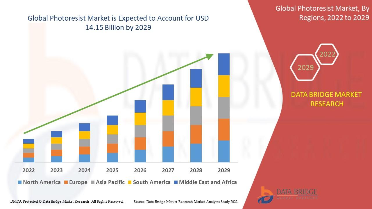
- The photoresist market was valued at USD 9.18 billion in 2021 and is anticipated to grow to USD 14.15 billion by 2029, with a CAGR of 5.55% over the forecast period of 2022–2029. The Data Bridge Market Research team’s thorough expert research, import/export analysis, price analysis, production consumption analysis, and climate chain scenario are all included in the market study.
- Technological advancement and semiconductor-related research and development have both grown over the past several years. The European Semiconductor Business Association (ESIA) estimates that the European semiconductor market earned US$3.8 billion in sales in May 2021, an increase of 31.2% from May 2020. The increase in semiconductor manufacture is driving the photoresist market’s expansion. As a consequence, over the duration of the projection, growth in the photoresist market is anticipated to be fueled by expansion in the semiconductor industry.
Key Trends –
The main market trend is said to be improvements in material technology. In the electronic sector, a novel strategy called direct wire technology is being used. It produces 3D lithographic patterns in a range of nanoparticle materials, including metal, semiconductor, insulator, and magnetic materials, using direct incident beam lithography. Direct incident lithography has several benefits, including rapid and simple patterning, a diversity of writing modes, a large number of applications, and high flexibility and usefulness in nano/microfabrication. In addition, the switch from MEMS to bio-NEMS/MEMS is limiting the development of the most advanced materials for patterning that use photoresist and related technologies. As a result, with the commercialization of such materials and products, the market for photoresists and related goods will have numerous opportunities.
For more detailed information about photoresist market
https://www.databridgemarketresearch.com/reports/global-photoresist-market
About Us
Leading worldwide technology research and advising firm Data Bridge Market Research. Their in-depth market trend research and analysis provide useful information that firms can use to spot market opportunities and create winning plans to strengthen their positions in the marketplace. The data bridge market research report collection has over 500 specialised analysts and currently has over 21000 publications covering. Businesses of various sizes, including more than 100 Fortune 500 corporations, make up their clientele. This expanding clientele base relies on data bridge market research’s thorough coverage, in-depth analysis, and practical industry insights to find opportunities in current and future markets and evaluate their competitive positions in dynamically shifting market environments.